Via in pad PCB
|
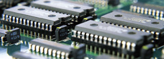
With the development of electronic products to the light, thin and small, PCBs are also pushed into high density, high difficulty. Among them, via in pad is one of the topics that engineering designer can not avoid. It is a main part of multi-layer PCB and directly helps to save PCB real estate up to 50% for fine pitch BGA and flip chip components. The main difficulty for the plugged via is to prevent soldering tin into via or solder mask onto pads. The accumulation of years of manufacturing experience has given us a good control on the PCB quality. |
|
|
|
|
Bicheng has been providing multilayer BGA via-in-pad printed circuit boards for electronics manufacturers, IT research organizations and universities, large or small, for the applications of communication systems, mobile terminal, computer and peripherals etc. |
|
|
|
|
It includes: |
|
|
FR-4 material:FR-4 TG>135, High TG 170, High CTI 600V |
|
|
Material Brand:ITEQ, SHENGYI |
|
|
Multilayer lamintion:In house |
|
|
Solder mask:Green, Blue, Yellow, Black, Red and its relative Matt color |
|
Surface finish:HASL Lead free, ENIG, Immersion silver, Immersion tin. |
|
via filling material:non-conductive epoxy resin |
|
|
via plugged:pad plugged flatly, good for next SMT process |
|
|
Product services:Prototypes, small volume and large production |
|
|
Freight services:Door to door, To sea port, To Airport service |
|
|
|